Modelos em alta
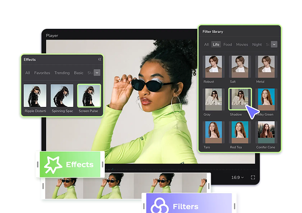
Free visualização 3d kicad Templates by CapCut
Add new video
00:16
8
Reflexão

00:09
19.6k
#Instagram

00:14
13.7k
Tem certeza?

00:04
16
3D Livewallpaper
00:19
475
Miniatur 3d viral
conversão fbx para obj
urso de pelúcia 3d
obj 3d gratuito
desenho 3D no AutoCAD

00:15
411
magic painting

00:08
329.1k
Um chupa cabra? kkkk

00:16
126.5k
Você deixou saudades

00:08
230.7k
my preview 2

00:14
1.5k
jornal nacional meme

00:08
19.5k
search

00:09
6.7k
Chuyển cảnh intro

00:13
356
modelo

00:11
28.0k
Sua Miniatura 3D

00:09
2.7k
Crie seu AVATAR

00:15
21.3k
os 4 caras